Precision meets power, it’s the regulator
With some caveats, this usually works, which is why references are continually expected to address increasingly higher current applications. After all, if the reference can power the converter, why not the analog signal chain, or another converter and the list grows–and why not?
There are many times in the design process where there is a decision between precision and power. The brute force approach suggests using a reference when precision is demanded, and a regulator whenever milliwatts of power are demanded. Besides the additional board space and cost, separate signals must be routed, even if their nominal voltages are the same. And, if a high precision voltage source is required to provide milliwatts of power, the designer is forced to buffer a reference. The LT6658 solves this dilemma by providing two low noise precision outputs with a combined 200mA output current and world class reference specifications.
General overview

The LT6658 is a precision low noise, low drift regulator with the accuracy specifications of a reference and the power of a linear regulator. The LT6658 boasts 10ppm/°C drift and 0.05% initial accuracy. On the power side the LT6658 has two outputs providing 150mA and 50mA each with 20mA active sinking capability. To maintain accuracy, load regulation is 0.1ppm/mA. Line regulation is typically 1.4ppm/V when the input voltage supply pins are tied together and less than 0.1ppm/V when the input pins are provided with independent supplies. To get a better understanding of the LT6658 features and how it works, a typical application is shown in Figure 1. The LT6658 consists of a bandgap stage, a noise reduction stage and two output buffers. The bandgap and two output buffers are powered separately to provide exceptional isolation. Each output buffer has a Kelvin sense feedback pin for optimum load regulation.
The noise reduction stage consists of a 400W resistor with a pin provided for an external capacitor. The RC network acts as a low pass filter band-limiting the noise from the bandgap stage. The external capacitor can be arbitrarily large reducing the noise bandwidth to a very low frequency.
Sourcing & sinking
As a regulator, the LT6658 supplies 150mA from the VOUT1_F pin, 50mA from the VOUT2_F pin and both pins sink 20mA. Active sinking capability helps to provide excellent transient response and permit fast settling. The transient response is short, while excellent 0.1ppm/mA load regulation is maintained.
Output tracking
For applications with multiple converters using different voltage references, the LT6658 outputs track, even if the outputs are set to different voltages, ensuring consistent conversion results. This is possible, because the two outputs of the LT6658 are driven from a common voltage source. The output buffers are trimmed resulting in excellent tracking and low drift. As the load on VOUT1_F increases from 0 to 150mA the VOUT2 output changes less than 12ppm. That is, the relationship between the outputs is well maintained even over varying load and operating conditions.
Power supply rejection & isolation
To facilitate exceptional power supply rejection and output isolation, the LT6658 provides three power supply pins. The VIN pin supplies power to the bandgap circuit while VIN1 and VIN2 supply power to VOUT1 and VOUT2, respectively. The simplest approach is to connect all three supply pins delivering a typical DC power supply rejection of 1.4ppm/V. When the power supply pins are connected separately and the VIN1 supply is toggled, the DC line regulation for VOUT2 is 0.06ppm/V. The VIN supply has the most sensitivity causing a typical 1.4ppm/V change on the outputs. Supply pins VIN1 and VIN2 have almost no effect.
The well isolated output buffers reject load transients from the adjacent buffer resulting in minimal effect on the adjacent output. Figures 2a and 2b illustrate channel-to-channel output isolation. One output is wiggled at 50mVrms, and the change in the adjacent buffer is plotted.

Power management & protection
The three supply pins help to manage the amount of power dissipated in the package. When supplying a large current, lower the supply voltage to minimize the power dissipation in the LT6658. Less voltage will appear across the output device resulting in less power consumption and higher efficiency.
An output disable pin, OD, turns off the output buffers and places the VOUT_F pins in a high impedance state. This is useful in the event of a fault condition. For example, a load may become damaged and shorted. This event can be sensed by external circuitry and both outputs can be disabled. This feature can be ignored and a weak pull-up current will enable the output buffers when the OD pin floats or is tied high.
The LT6658 comes in a MSE-16 exposed pad package with a qJA as low as 35°C/W. When the supply voltage is high, the power efficiency will be low resulting in excessive heat in the package. For example, a 32.5V supply voltage at full load with have 30V*0.2A of excess power across the output devices. The total amount of excess power is 6W which will raise in the internal die temperature 210°C above ambient temperature! To protect the part, a thermal shutdown circuit will disable the output buffers when the die temperature exceeds 165°C.
Noise
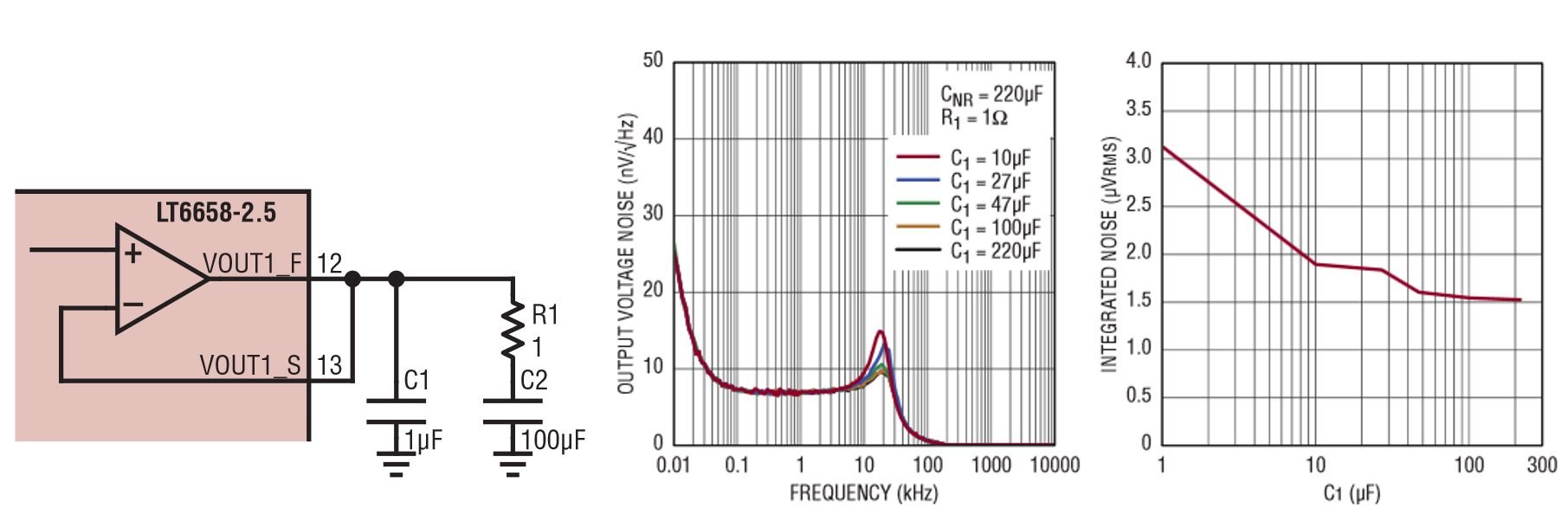
For data converter and other precision applications, noise is an important parameter. The low noise LT6658 can be made even lower with the addition of a capacitor on the NR (noise reduction) pin. A capacitor on the NR pin forms a low pass filter with an on-chip 400W resistor. A large capacitor lowers the filter frequency and subsequently, the total integrated noise. The left part of figure 3 shows the effect of increasing the values of the capacitor on the NR pin. With a 10μF capacitor the noise rolls off to about 7nV/ÖHz.
By increasing the output capacitor, the noise can be further reduced. When both the NR and output capacitors are increased, the output noise can be reduced down to a few microvolts. The LT6658 is stable with output capacitance between 1μF and 50μF. The output is also stable with large capacitance, if a 1μF ceramic capacitor is placed in parallel. For example, the center of figure 3 shows a circuit with 1uF ceramic capacitor in parallel with a 100uF poly-aluminum capacitor. This configuration remains stable while lowering the noise bandwidth. The right part of figure 3 illustrates the noise response for different values of output capacitance. In all three cases, there is a small 1uF ceramic capacitor in parallel with the larger capacitor.

One drawback of this scheme is the noise peaking which can add to the total integrated noise. To reduce the noise peaking a 1W resistor can be inserted in series with the large output capacitor as shown in the left part of figure 4. The output voltage noise and total integrated noise are shown in the center and right parts of figure 4, respectively.
Applications
The LT6658 can provide quiet precise power for a number of demanding applications. In the mixed signal world, data converters are often controlled by microcontrollers or FPGAs. Sensors provide signals to analog processing circuits and converters, all of which need clean power supplies. The microcontroller may have several supply inputs including analog power. As a general rule, noisy digital supply voltages for the microcontroller should be isolated from the clean precise analog supply and reference. The two outputs of the LT6658 provides excellent channel-to-channel isolation, power supply rejection and supply current capability, ensuring clean power to multiple sensitive analog circuits.
The LT6658 is also well suited to industrial environments with its ability to operate with noisy supply rails and where load glitches due to conversions on one output have very little influence on the adjacent output. Moreover, when a load demands current on one output, the adjacent output continues to track.
The circuit in Figure 5 illustrates how the LT6658 can power noisy digital circuits, while maintaining a quiet precise reference voltage for a precision ADC.

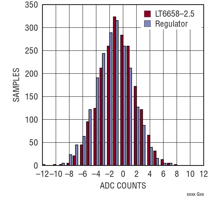
In this application, the LT6658 or a separate regulator supplies power to a 3.3V rail driving a noisy FPGA supply (VCCIO) and some miscellaneous logic on one channel, and 5V to the reference input of the 20-bit ADC on the other channel. By switching the digital supply between the LT6658 and the regulator, we can assess how well the LT6658 can isolate digital noise on one channel from the channel driving the quiet reference input of the 20-bit ADC. Using a clean DC source on the input of the ADC, the noise can be inferred as shown in Figure 5b. The histogram does not appreciably differ whether the LT6658 or when the regulator supplies power to the VCCIO pins of the FPGA, demonstrating the LT6658’s robust regulation and isolation.
Conclusion
The LT6658 is the next step in the evolution in the world of references and regulators. The precision performance and ability to provide a combined 200mA of current from a single package is a paradigm shift for precision analog power. Noise rejection, channel-to-channel isolation, tracking, and load regulation put this product squarely in the path of tomorrow’s precision analog reference and power solutions. With this new approach, applications will not have to compromise precision or power.
About the author:
Michael B. Anderson is Senior Design Engineer, Signal Conditioning Product Group at Analog Devices – www.analog.com
 If you enjoyed this article, you will like the following ones: don't miss them by subscribing to :